RF Building Blocks
CMX998 – Cartesian Feedback Loop Transmitter
A Cartesian Feedback Loop (CFBL) Transmitter improves the efficiency and linearity of transmitters for non-constant envelope modulation systems. The CMX998 is an integrated solution for a linear based Cartesian Feedback Loop (CFBL) transmitter. Acting as a direct conversion quadrature mixer from I and Q to RF output, it provides the capability to linearise the Power Amplifier (PA) via feedback from the PA’s output. Included are forward and feedback paths; local oscillator circuitry including loop phase control; an instability detector and uncommitted op-amps for input signal conditioning. The differential inputs are ideal for direct connection to standard modems and interface ICs such as CML’s CMX7163 QAM Data Modem, CMX983 Analogue Front End (AFE) for Digital Radio, CMX7364 Multi-mode High Performance Modem and more!
Devices are available through our Distributor Network.

Features
- Frequency Range: 30MHz to 1GHz
- Wideband Noise: -148dBc/Hz
- C-BUS (SPI Compatible) Serial Interface
- Gain Control, Error Amplifier
- Up-Converter Forward Path
- Down-Converter for Feedback Linearisation
- 360 Degrees Loop Phase Shift Control
- DC Offset Measurement Output
- Open-Loop Function, Instability Detector
- Linearisation Gains of 30dB or more Achievable
- Flexible Digital Interface
Applications
- TETRA/TETRA2 Terminals
- APCO P25 Phase 2
- Software Defined Radio (SDR)
- Aviation Systems
- Mobile Satellite Terminals
- Linear Modulation Schemes: QPSK, pi/4 DQPSK, 8PSK, QAM, OFDM, F4FM
Power Supply Requirement
- 3.0 to 3.6 V power supply
Design Resources
CMX998
Q. What is the specification for the accuracy of the CMX998 transmitter in terms of I/Q phase and amplitude balance?
A. The modulation accuracy of a CMX998 transmit is determined by the down-converter (feedback path).
The I/Q amplitude and phase balance of the down-converter is therefore the key factor in determining the contribution the CMX998 makes to a transmitters modulation accuracy.
In practice it doesn’t matter if the I/Q error is an amplitude imbalance or a phase imbalance, it is the total error that is important.
For this reason the CMX998 specifies the I/Q phase and amplitude balance as a composite in terms of ‘Feedback path Image Suppression’.
A worst-case value of –30dB is guaranteed.
The parameter can be calculated from I/Q phase and amplitude balance using the following formula:
Image Suppression / dBc = 10*log[((k^2+1)-2*k*cos(theta)) / ((k^2+1)+2*k*cos(theta))]
Where: k = amplitude balance (linear I/Q ratio
Select I/Q or Q/I for ratio = <1)
theta = phase balance
Q. Can the CMX998 be used for TETRA 2?
A. Yes, the CMX998 meets the linearity and wideband noise requirements of TETRA QAM modes for 25kHz, 50kHz, 100kHz and 150kHz channels.
Note that a different loop-filter might be required for the 100kHz and 150kHz channels.
Q: How do I control the CMX994 or CMX998 on the DE9941 board?
A: The DE9941 includes the CMX7164 Multi-Mode Modem, the CMX998 Cartesian Feedback Loop Transmitter, and the CMX994 Direct Conversion Receiver. When the PE0003 Ev Kit Interface Card is used as the host controller for DE9941, the PE0003 communicates with the CMX998 and CMX994 through the CMX7164’s SPI Thru-Port. The CMX7164 SPI Thru-Port is beneficial because it allows control of peripherals with fewer uC pins and PCB traces.
There are three CMX7164 internal registers that are key for this discussion:
– $62, SPI Thru-Port Control
– $63, SPI Thru-Port Write
– $78, SPI Thru-Port Read
CMX7164 register $78 comes into play when you need to read an external device register. CMX7164 register $63 contains the value to be written to an external device register, and CMX7164 register $62 defines important C-BUS/SPI parameters such as:
– Which Chip Select will be used for the transaction
– If the transaction will be read or write
– Number of bytes to be written to the target device
– CMX7164 IRQ behavior when the write is completed
– The address of the target device
For example, let’s say we need to write 0xFC to CMX998 register $02 using the CMX7164 SPI Thru-Port. Pseudocode of the required SPI Thru-Port transaction would look like this:
– Host writes 0xFC to CMX7164 register $63
– Host then writes 0x4102 to CMX7164 register $62 (SSOUT1, Interrupt when the C-BUS Thru-Port Control/Write registers are free, write transaction, 1 data byte, register address $02)
To do this same transaction in the PE0003 graphical user interface (GUI):
– Select “C-BUS Control” tab and observe the “Write a Register” area
– Ensure “16 bit” is checked
– Enter 63 for “Register Address”, enter FC for “Register Data”, and then click “Write”
– Enter 62 for “Register Address”, enter 4102 for “Register Data”, and then click “Write”
Here is a pseudocode example of a read transaction using the SPI Thru-Port. In this example, CMX998 “readback” register $F2 will be read out:
– Host writes $71F2 to $62 (SSOUT1, Interrupt when read or write operation triggered by this Thru-Port command is completed on the SPI port, read transaction, 1 data byte, register address $F2)
– Host waits for IRQ
– Host reads CMX7164 register $78 to obtain the data
To do this same transaction in the PE0003 GUI:
– Select “C-BUS Control” tab and observe the “Write a Register” area
– Ensure “16 bit” is checked
– Enter 62 for “Register Address”, enter 71F2 for “Register Data”, then click “Write”
– Move over to the “Read a Register” area
– Enter 78 for “Register Address”, then click “Read”. The data will appear in the grayed-out data box.
Control of the CMX994 Direct Conversion Receiver is performed in the same manner.
When using the CMX998 Cartesian loop IC with its evaluation kit (EV9980) I have seen degradation in carrier leakage when I enable the RF detector after the DC calibration phase.
What can I do to ensure a stable carrier leakage when I enable the RF detector?
A. In some configurations of the EV9980 the DC offset adjustment appears degraded when DCMEAS is set to “0” to “1”.
That is to say when the RF detector output is connected to the DCMEAS pin following a DC calibration procedure. The cause of this is internal offsets that result in a small, (nominally 5mV), shift in VREF and BVREF when the change is made.
The effect is shown in Table 1 (below):
|
DC On |
RF Det. |
DCMEAS |
Carrier leakage with DC offset adjusted on |
Carrier leakage with DC offset adjusted on |
|
1 |
0 |
0 |
-33dBm (-63dBc) |
-26dBm (-56dBc) |
|
1 |
1 |
0 |
-33dBm (-63dBc) |
-27dBm (-57dBc) |
|
0 |
1 |
0 |
-24dBm (-54dBc) |
-27dBm (-57dBc) |
|
0 |
1 |
1 |
-4dBm (-34dBc) |
-22dBm (-52dBc) |
|
1 |
1 |
1 |
-4dBm (-34dBc) |
-22dBm (-53dBc) |
|
0 |
0 |
1 |
-23dBm (-53dBc) |
-28dBm (-58dBc) |
Table 1 – Carrier leakage achieved with for various conditions of DCMEAS and associated control signals, PA enabled (+30dBm mean power with modulation), 450MHz, Divide by 2 LO
The transmitter is configured for +30dBm mean output power, TETRA pi/4-DQPSK or two-tone modulation, so a carrier null of ?33dBm is -63dBc, where ‘c’ is based on the mean signal power.
When DCMEAS = ‘1’ and the RF detector is enabled a degradation in carrier offset is observed with a previously adjusted carrier null. This issue can be greatly reduced if the alternative configuration for applying a bias voltage to the input signal is used, as documented in EV9980 Datasheet version 5 and above.
With PCB555D in ‘Mod State’ 3 or 5 the BVREF signal is used to bias the input signal. This means a common shift is applied to DC offset correction signal and modulator reference.
The results from this improved configuration are also shown in Table 1 and although a small degradation is still observed the carrier leakage is still -52dBc, which is considered more than adequate for most applications.
For clarification, the relevant change is: R5=5k1 (formerly NF) R7=NF (formerly 20k), R53=NF (formerly 20k), R57=5k1 (formerly NF).
This change can be applied to PCB555C and well as PCB555D.
Notes:
1. PCB555C (all ‘Mod States’) and PCB555D ‘Mod States’ 2 and 4.
2. PCB555D ‘Mod States’ 3 and 5.
Q. Can you help explain how the instability detector on the CMX998 operates and how it can be used?
A. The instability detector found on the CMX998 is a relatively simple mechanism that measures the level of out-of band energy of the feedback loop.
If the loop becomes unstable due to phase inaccuracies the feedback loop will tend to spill energy out-of band.
The instability detector comprises a high-pass filter followed by a peak-detector circuit and this combination indicates the presence of this high frequency energy.
As phase error increases, the instability detector will show a worsening level of out-band energy.
The classic behaviour of the Cartesian loop is for the output band energy to ‘peak’ close to the edge of the loop-bandwidth. This ‘peak’ will occur at -ve frequency or +ve frequency depending on whether the phase error is a lead or a lag.
Note: The CMX998 instability detector cannot detect lead or lag error as it works on a simple baseband signal.
The error signal produced by the instability detector should be accessed for a particular design and an appropriate threshold set.
The CMX998 includes gain adjustment to make threshold setting easier.
Note: If the loop is set up 180 degrees out of phase the loop will oscillate and will generally produce a maximum level carrier.
As this is effectively a stable oscillating condition the instability detector will not detect this operating state.
The instability detector is designed to detect minor phase variations and resultant instability following initial phase correction.
Typical changes are variations in antenna VSWR and thermal effects. Such effects are unlikely to cause a phase shift as large as 180 degrees.
If instability is detected, then normal procedure is to power down the transmitter. If a design supports dynamic loop phase calibration, then an instability detector event normally triggers loop re-calibration.
CMX998 with an RF5110G Power Amplifier
This document is intended as an aid to customers developing linear transmitters using the CMX998 integrated circuit by demonstrating a typical ‘Cartesian Loop’ transmitter solution using ‘off-the-shelf’ components.
CMX998 Cartesian Feedback Loop DC Calibration
This Application Note is intended as an aid to customers developing linear transmitters using the CMX998 Cartesian Feedback Loop IC. This IC allows the implementation of an analogue Cartesian feedback loop (CFBL) around a power amplifier (PA).
CMX998 - Exploring High Data Rate Applications
This Application Note details measurements made using a CMX998 in a TETRA 2 system both as a proof of concept for TETRA 2 applications and for wideband applications in general.
DE9941 in TDMA systems
Using a Cartesian transmitter in TDMA systems can be challenging when supporting multiple modulation formats. This App Note discusses these issues using the DE9941 in a worked example
View
CMX7164 2FSK 4FSK RAW Scripts
The two scripts contained in the ZIP file demonstrate the use of 2/4FSK transmitting and receiving up to 7 million bits of raw data through an RF wireless link. These scripts require the following evaluation boards: Two x PE0003, Two x PE0601-7164, One x EV9980, One x EV9920B. It is important to read the included readme.txt file. It is recommended that you read the QAM + RF Demonstration application information and watch the YouTube video for the Full QAM + RF Demo" as the setup of the evaluation boards is the same.
View
PE0601-7164 - 2FSK 4FSK Formatted Scripts
The two scripts contained in the ZIP file demonstrate the use of 2/4FSK transmitting and receiving Block 2 Formatted data through an RF wireless link. The Data frame consists of Header Block, Intermediate Block and Last Block. These scripts can be easily modified to support other Block Types. These scripts require the following evaluation boards: Two x PE0003, Two x PE0601-7164, One x EV9980, One x EV9920B. It is important to read the included readme.txt file. It is recommended that you read the QAM + RF Demonstration application information and watch the YouTube video for the Full QAM + RF Demo" as the setup of the evaluation boards is the same.
View
DE9941 Demonstration
DE9941 Demonstration: Three scripts for evaluating performance of a multi-mode modem using the DE9941. Please refer to the Included Application Note and the DE9941 User Manual for a description of these scripts and their operation.
View
| DE9941A | 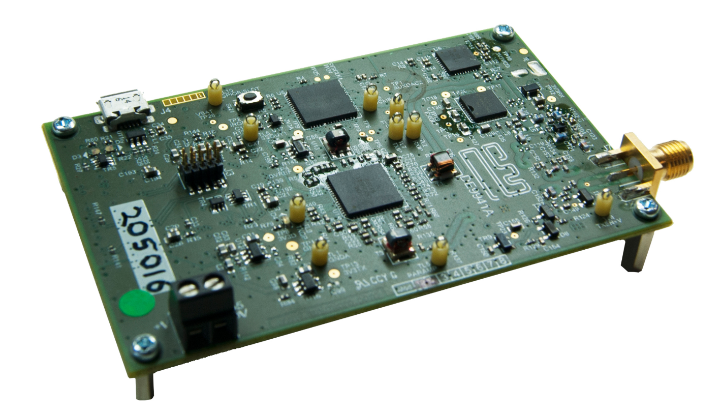 |
The DE9941A is a credit-card sized, fully functional, UHF wireless data modem using the CMX994E Direct Conversion Receiver, the CMX998 Cartesian Feedback Loop Transmitter and the CMX7364 High Performance Multi-mode Wireless Data Modem. Full design data and test scripts are available to download from the DE9941A Product Page. | DE9941A_Product_Page |
| EV9980 | 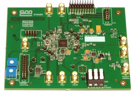 |
The EV9980 EvKit allows rapid and full evaluation of the CMX998 Cartesian Feedback Transmitter IC. In the form of a populated PCB, this flexible platform enables users, using a control interface, to configure and evaluate the CMX998 to various applications and frequency bands. | EV9980_Product_Preview
|
C-BUS Guides
Guides to operation and interfacing
EV9980 Schematic
EV9980 high resolution schematics and component overlay. Version D05
EV9980 Evaluation Software
A common GUI-based application for the EV9980 Evaluation Kit. A PE0003 Universal Interface Card is required to use this application. Version 5.1
EV9980 Quick Start
A simple guide to help users get started evaluating the EV9980. Version 1
PE0003 Driver
PE0003 USB driver for Windows. Version 1.0
DE9941 Board Schematics
DE9941BoardSchematics. Version BO5
DE9941 - PCB files
Evaluation board design files and schmatics for P-CAD and Excel BOM. See readme.txt. Version B05
DE9941 Quick Start
A simple guide to help users get started evaluating the DE9941. Version 1
CMX998 Noise Calculator
A tool to estimate the noise floor of a Cartesian loop control system using the CMX998. The theory of operation and detailed instructions for use are included in the download.