Maritime Communications
CMX7032/CMX7042 – AIS Baseband Processor ICs (with embedded exactTrax™)
The CMX7032 and CMX7042 are highly integrated baseband signalling processor ICs that fulfill the requirement of an SOTDMA and CSTDMA AIS transceiver, dual AIS Receive only device and exactTrax™ and exactSeNS long range AIS Class-B tracking.
These devices provide a quick route to developing an AIS based system and getting to market fast. Embedding much of the AIS, DSC and exactTrax™ protocol ensures minimal host involvement, therefore the designer can concentrate on the overall end application. Built on FirmASIC® technology, the CMX7032/CMX7042 provide the ultimate flexibility when designing Marine AIS based systems. The latest function image (7032FI-3.1.0.3) adds support for exactEarth’s new exactSeNS service. This provides a data payload capability within dedicated ASM-based messages transmitted using sophisticated encoding to support reliable reception via satellite and provides a core building block to enable the expansion of Marine IoT solutions.
Three function Images are available, these can be downloaded from the CML Technical Portal (contact for access):
- CMX7032/7042FI-1.x – AIS class A/B transceiver operation (CSTDMA/SOTDMA)
- CMX7032/7042FI-2.x – Low cost autonomous AIS dual receiver operation
- CMX7032/7042FI-3.x – exactTrax™/exactSeNS + AIS class B transceiver operation
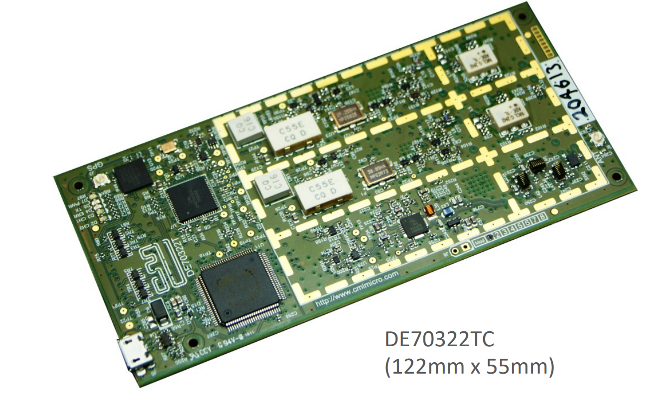
Please note: The SCT7033 is a complete, proven, protocol solution that seamlessly integrates with the CMX7032. The DE70322TC is a complete AIS Class B CSTDMA (IEC 62287-1) technology demonstrator/reference design package for use with the SCT7033.
Devices are available through our Distributor Network.

Features
- GMSK and FSK Modem
- Marine AIS and DSC data formatting
- exactTrax™ and exactSeNS long range operation and formatting
- Supports CSTDMA/SOTDMA operation
- Configurable by Function Image™
- Optimum co-channel performance
- Flexible signal channels:
– Two simultaneous Rx
– One Tx - Two flexible Integer-N Synthesisers (CMX7032 only)
- Two synthesised PLL clocks
- Limiter-discriminator Rx interface
- Flexible Tx interface
– I and Q
– Two Point Modulation - Auxilary ADC and DAC Functions
– Four x 10-bit DACs
– Two x 10-bit ADCs
Applications
- AIS class A transceivers
- AIS class B transceivers
- exactTrax™ and exactSeNS long range AIS tracking
- Marine AIS Rx-only
- AIDS to Navigation (AtoN)
- Marine AIS Search and Rescue Transponder (SART)
Power Supply Requirement
- 3.3V
Design Resources
CMX7032 and CMX7042 FAQ
Function Image™ Loading Options
Q. I am about to start a design using one of your FirmASIC® based products, what is the most suitable method of storing the associated Function Image™ in my project?
A. Our FirmASIC® based devices require a Function Image to configure their On-chip sub-systems.
This data file is uploaded during device initialisation and defines the device’s function and feature set.
The Function Image can be loaded automatically from external serial memory or from a host µController over the C-BUS/SPI port. The serial memory can be programmed using a dedicated programmer.The serial memory can also be programmed using the target CMX7xxx device and the host processor. This facility makes programming the serial memory possible during factory test or through field upgrade.
-The method for loading an FI over C-Bus/SPI is detailed in the device’s data sheet.
-The method for programming the serial memory is described in this application note.
For FI-2.x only. Directions for loading an FI over the RS-232 port can be found here.
For CMX7032 FI-2.x
Q. The CMX7032 FI-2.x includes a NRESET pin, I understand that this allows the device to be fully reset following a temporary loss of power (e.g. Brown Out Condition).
Is there a particular way to use this pin if I am using an external Serial memory to store the Function Image?
A. The hyperlinked pdf document CMX7032 Power up and reset provides an illustration of how the NRESET can be used during a Brown Out Condition.
It can be used at any time following an initial [power up sequence and Function Image load).
CML recommends the use of an external voltage supervisor IC if it is exposed to variable supplies such as those found in automobile applications.
For CMX7032FI-1.x/2.x/3.x and CMX7042FI-1.x/2.x/3.x
Q. I am about to evaluate the AIS Baseband Processor what Evaluation Kit is recommended?
A. For RF evaluation, the DE70322T provides a complete solution and is offered as a demonstration module / reference design.
- The DE70322T is a complete solution for a high quality, standalone AIS receiver.
- The DE70322T with the PE0003 for evaluation using FI-1.x or FI-2.x in AIS receivers.
- The DE70322T with the PE0003 for evaluation using FI-1.x and FI-3.x in AIS Class B transceiver designs.
For evaluation at baseband, either the PE0201 or PE0401 kits are the best option. These kits can be used with RF test sets or vector generators and signal analysers. The tx and rx channels require a relatively flat frequency response that extends near to dc.
For 7032FI-1.x or 7032FI-3.x use the PE0201 kit with the following changes:
- C21 and C22 on the Mod1 and Mod2 paths should be removed
- C11 at the discriminator input must be replaced by a zero ohm link
- The removal of C17 may also benefit performance
- All other components may remain the same
For 7042FI-1.x use a PE0402 kit where solder pads are provided to allow a solder bridge to be made in series with each input decoupling capacitor. The outputs are already dc coupled so no further changes are required. See the PE0402 User Manual and schematic.
DSC decode in dual DSC/AIS receiving mode
Q. I have enabled both DSC and AIS burst decoding following the Data Sheet description. AIS messages are received correctly but I do not receive any DSC messages.
A. If mixed AIS and DSC channels are to be used then DSC can be assigned to either Rx1 or Rx2 but the AIS receive task must be started before the DSC receive task is started. If only DSC is selected, then it can be assigned to either Rx1 or Rx2 and started normally.
For Rx1 DSC and Rx2 AIS channel reception:
$C1 = $0001 ; select DSC on Rx1 and AIS on Rx2
$C8 = $0001 ; reset Rx1
Wait for com reg free flag to be set
$C8 = $0005 ; reset Rx2
Wait for com reg free flag to be set
$C8 = $0006 ; enable Rx2, AIS Formatted mode started before DSC formatted mode
Wait for com reg free flag to be set
$C8 = $0042 ; enable Rx1, DSC Formatted mode
For Rx1 AIS and Rx2 DSC reception:
$C1 = $0002 ; select DSC on Rx2 and AIS on Rx1
$C8 = $0001 ; reset Rx1
Wait for com reg free flag to be set
$C8 = $0005 ; reset Rx2
Wait for com reg free flag to be set
$C8 = $0002 ; enable Rx1, AIS Formatted mode started before DSC formatted mode
Wait for com reg free flag to be set
$C8 = $0046 ; enable Rx2, DSC Formatted mode
CMX703x/CMX704x Writing a Function Image File to Serial Memory
Writing a Function Image File to Serial Memory
CMX7032 How to set and use the RSSI and CS features
How to set and use the RSSI and CS features of the CMX7032FI-1.x
CMX7032/42 - RX1 Channel DSC Data Burst Reception
Receive DSC data bursts on RX1 using the PE0201/PE0402 and PE0003 Ev Kits. The data length and RX State errors are saved to a file "RX1 DSC Burst". The download includes a wav file that generates 3 DSC bursts for testing DSC receivers.
View
CMX7032/42 - Dual Channel AIS Burst Reception
Receives AIS data bursts on RX1 and RX2 using the PE0201/PE0402 and PE0003 board. Saves data length, dc offset, Time of Arrival, AIS data and RX State errors to file.
View
CMX7032/42 - Channel 1 AIS Burst Reception
Receive AIS data bursts on RX1 using the PE0201/PE0402 and PE0003 boards. Saves data length, dc offset, Time of Arrival, AIS data and Rx State errors to file.
View
CMX7032/42 - Channel 2 AIS Burst Reception
Receive AIS data bursts on RX2 using the PE0201/PE0402 and PE0003 boards. Saves data length, dc offset, Time of Arrival, AIS data and Rx State errors to file.
View
PE0003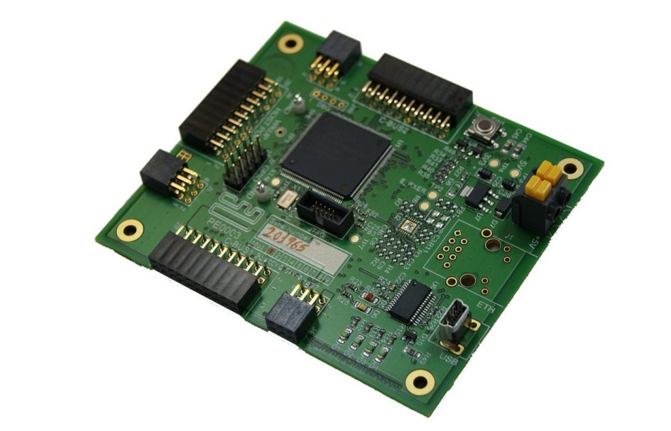 |
The PE0003 Evaluation Kit Interface Card is a global interface system for use with evaluation kits for CML’s new generation ICs, including FirmASIC™ based products. This greatly simplifies the approach to the evaluation and design-in process. | PE0003_Product_Page |
PE0402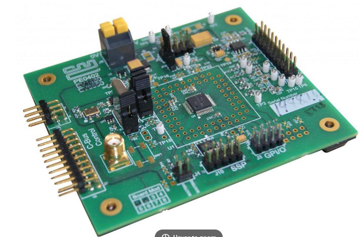 |
The PE0402 Platform Evaluation Kit is designed to assist in the evaluation and application development of the CMX704x/CMX714x range of FirmASIC products. | PE0402_User_Manual
|
| DE70322T
|
The DE70322T is a complete AIS Class B (IEC 62287-1) technology demonstrator/reference design package that will enable manufacturers to quickly deploy an AIS Class B transceiver to the market. | DE70322T_Product_Page |
White Paper: Marine AIS
White Paper: Marine AIS
CMX7032 FI-2.x test wav
A wav recording of the Eddystone message described in the CMX7032 User Manual. This file can be used to test the baseband receiver of the CMX7032 or modulated to RF and used as test signal.
Download
C-BUS Guides
Guides to operation and interfacing
exactTrax™ Whitepaper
Introduction to exactTrax™ technology