Digital/Analogue Two-Way Radio Products
CMX7031/CMX7041 – Two-way Radio Processor IC Offering Voice, Signalling and Data Functions
The CMX7031 and CMX7041 are half-duplex radio processor IC platforms using FirmASIC technology, that are suitable for use in multi-standard analogue Two-way Radio (TWR) systems.
FirmASIC component technology allows on-chip sub-systems to be reconfigured by a Function Image (FI): this is a data file that is uploaded during device initialisation that defines the device’s function and feature set.
The CMX7031/CMX7041 enable a revolutionary new platform approach to radio design, enabling multi-mode analogue two-way radios to be developed based on a single radio platform, conforming to many systems: PMR, LMR, Trunking, Marine, Aviation, Amateur radio, NOAA weather radio and packet data radio.
Four Function Images are available, these can be downloaded from the CML Technical Portal (contact for access):
- CMX7031/7041 FI-1.x – Baseband Audio and Data Processor with Auxiliary System Clocks, ADCS and DACS for use in Analogue Radio Systems
- CMX7031/7041 FI-2.x – 4LFSK Baseband Data Processor with Auxiliary System Clocks, ADCs and DACs
- CMX7031/7041 FI-3.x – C4fm Baseband Data Processor with Auxiliary System Clocks, ADCs and DACs
- CMX7031/7041 FI-4.x – AX.25 Modem (1200bps AFSK and 9600bps GMSK) with Auxiliary System Clocks, ADCs and DACs for use in Amateur Packet Radio
Click the links above or visit the "Downloads" section of this page to download the datasheets for each individual Function Image.
Devices are available through our Distributor Network.

Features
7031/7041FI-1.x:
- Full Audio Baseband Processor with Selectable Processing Order
- Voiceband and Sub-audio Signalling
- 1200/2400 bps FFSK/MSK Freeformat Data
- NOAA and NWR Operations
7031/7041FI-2.x:
- 4.8 and 9.6 kbps 4-Level FSK Data with Freeformat and Packet Modes
7031/7041FI-3.x:
- 4.8 and 9.6 kbps C4FM Data with Freeformat and Packet Modes
7031/7041FI-4.x:
- 1200bps AFSK Modem
- 9600bps GMSK Modem
Applications
- PMR and LMR Systems
- Trunked Radio
- Marine, Aviation and Amateur Radio
- National Weather Radio (NWR)
Power Supply Requirement
- 3.0 to 3.6 V
Design Resources
Function Image Available:
| Description | Function Image |
| Multi-mode Analogue TWR Processor | 7031/7041FI-1.x |
| 4-level FSK Data Modem | 7031/7041FI-2.x |
| C4FM Data Modem | 7031/7041FI-3.x |
| Amateur Radio AX.25 Modem | 7031/7041FI-4.x |
7031/7041 FAQ
Tx and Rx FFSK Data Operations Q. Is there a recommended procedure for handling FFSK/MSK data in transmit or receive modes when using the CMX70x1 (7031/7041FI-1.3) Two-Way Radio Processor ICs? A. The linked pdf document provides an overview in the form of flow charts that illustrate which C-BUS registers need to be written-to and read-from when attempting a data transmission. It is indicative only and provides a minimum set of reads/writes to achieve successful data transfer.[CMX70x1 Tx and Rx FFSK Data Operations]
Function Image 1.x – Auxiliary ADCs Q. Are there any differences between the CMX70x1 FI – 1.x and the CMX88x series of devices in the way the AuxADC handles interrupts when a signal passes through the high and low threshold points? A. The threshold facility allows the relevant devices to trigger an interrupt when a signal exceeds the high threshold limit or falls below the lower threshold limit. This is a useful feature when trying to detect changes in received signal strengths or voice activity for example. These thresholds are programmable which allows a lot of flexibility when designing a system. Please note though that there is a subtle difference between the way the CMX70x1 FI – 1.x and the CMX88x series of devices handle the resultant interrupts. The following link will take you to an illustration of how interrupts are handled. [Auxiliary ADC Interrupts]
Scrambling Q. Can you give me any information on the use of scrambling when using these products? A. In order to achieve reasonable intelligibility of recovered scrambled/descrambled speech, the limitations detailed in the linked document should be considered. [Frequency Inversion Scrambling]
FI-1x Q. I am about to start to use the CMX7041 in an application that uses CTCSS and FFSK data, do you have a worked example or illustration that I can refer to? A. The following link will take you to a document that includes 4 basic examples both in transmit and receive. Signal paths and C-BUS register settings are shown for clarity. [view document]
FI-2x Q. I am about to evaluate the CMX70x1 FI2.0 (4FSK Modem) using the PE0201, what recommendations can you give me? A. Operation is straightforward when following the instructions in the user manuals and FAQs, however a modest modification to the PE0201 is recommended. The baseband signal requires a Tx-to-Rx channel with a relatively flat frequency response. To achieve this with the PE0201 kit from the default build will require the removal and replacement of certain capacitors.
- C21 and C22 on the Mod1 and Mod2 paths should be removed
- C11 at the discriminator input must be replaced by a zero ohm link
- The removal of C17 may also benefit performance
- All other components may remain the same
Note: If evaluating the 7041FI-2.x with a PE0401 kit the same modifications should be made.
FI-3.x modified: 11/05/07 Q. I am about to evaluate the CMX70x1 FI3.0 (C4FM Modem) using the PE0201 what recommendations can you give me? A. Operation is straightforward when following the instructions in the user manuals and FAQs however a modest modification to the PE0201 is recommended. The baseband signal requires a Tx-to-Rx channel with a relatively flat frequency response. To achieve this with the PE0201 kit from the default build will require the removal and replacement of certain capacitors.
- C21 and C22 on the Mod1 and Mod2 paths should be removed
- C11 at the discriminator input must be replaced by a zero ohm link
- The removal of C17 may also benefit performance
- All other components may remain the same
Note: If evaluating the 7041FI-2.x with a PE0402 kit the same modifications should be made.
Function Images Q. How long does it take to download a typical Function Image (FI) to a member of the CMX70xx family of devices? A. The largest factor in overall Function Image (FI) download time is the main sequence of writing words to the IC’s programming register ($C8). We will consider the repetitive nature of the recommended sequence in the linked illustration. We can see that: Download Time = FI word count x (TREAD + TWRITE + TMEM + TREG). Where:
- TREAD and TWRITE are largely determined by C-BUS sclk speed. Up to a maximum of 5Mbps
- TMEM is determined by host processor memory access time. Dependent on processor speed and latency etc. Much will depend on whether the host processor is only processing the FI download or not. Concurrent processing on the host is not recommended when downloading the FI.
- TREG is determined by the local clock or crystal source (and sys clock settings)
For a 6.144MHz clock we can approximate TREG ˜ 5.3us For a 19.2MHz clock we can approximate TREG ˜ 1.6us In evaluation it was shown that not using interrupts but polling the Status Register until the programming flag is set ($C6, b0), achieved best overall performance. This approach is further enhanced if the time taken by 8 x C-BUS sclk cycles is greater that the time taken for the CMX70xx to process a single prewritten Word. Or: 1/Sclk x 8 < TREG This process then takes advantage of the fact that the times TREAD and TREG are independent processes and can take place concurrently. The following link takes you to an illustration of this improved method. Example: Assume a maximum FI size of 23kWords, 2Mbps sclk, 6.144MHz clock source and a host processor latency of 10us. The calculation includes the improvement introduced by polling only (interrupt is masked) so TREG has been removed. Download Time = FI word count x (TREAD + TWRITE + TMEM) 1/Sclk x 8 = 4us which is less than 5.3us so the above equation is valid Therefore: Download Time = 23k x (12us + 12us + 10us) = 800ms Notes:
- Power cycling, resets of the CMX70xx will also add to the overall time. However under normal circumstances a FI re-write does not require power cycling a reset procedure will be sufficient.
- In practice real FI sizes will be less than the maximum 23Words, typical sizes will be half this figure. Please refer to the relevant FI pages on the CML web portal (My_CML).
Conclusion It can be seen that FI downloads can reliably be written in no more than a few seconds. Updating an existing FI with a new variant will take no longer than the initial install as the RESET procedure is very quick. The largest delay to FI installation potentially is the host processor latency and the speed at which the C-BUS sclk is driven.
Q. What are the NWR functions? A. A new feature is the provision of NWR, which allows customers in the USA to decode and respond to the NWR / NOAA weather broadcasts. The new signal processing architecture of the CMX7031/CMX7041 allows this signal to be decoded in parallel with the other PMR / FRS signal processing.
Q. What are the C-BUS differences between the CMX7031/CMX7041 and the 88x series? A. The CMX7031 and CMX7041 are based on the successful 88x series of devices but offer some significant improvements and many functional enhancements. The flexibility of the FirmASIC platform allows for further development and features can be added as required. Some changes have been made to the C-BUS host interface to accommodate the complete set of features from the 88x series and the additional features of the 7031, however, whenever possible, backwards compatibility has been maintained to ease the transition to the new family. The AuxADC/TX Mod Mode, Analog Output Gain and Input Gain registers ($A7, $B0, $B1) must be used to set up the Audio routing through the device. The Powerdown, Mode Control, Interrupt Mask and Interrupt Status registers ($C0, $C1, $CE, $C6) have been changed to support the new functionality. The sub-audio signalling (CTCSS and DCS) control and reporting has been rationalised to use the Audio Control and Tone Status registers ($C2, $CC). The In-band signalling has been expanded to include DTMF Rx and uses Tx In-Band tones and Tone Status registers ($C3, $CC). All In-band tones activity is signalled to the host via IRQ bit13 (this includes DTMF Rx). The frequency resolution of the Selcall and Custom tones has been improved, but the consequence is that the values used in the Program Registers are different from the 88x series. New Program block registers have been introduced to support the new and improved functionality.
FAQ and Applications Disclaimer Notice Information, or software, viewed or downloaded from the CML FAQ or Application Notes sections of the CML website is provided “as is” without warranty of any kind, either express or implied, including, but not limited to, the implied warranties of fitness for a purpose, or the warranty of non-infringement. CML reserves the right to make changes to the information available at any time and assumes no liability for applications assistance or customer product design. Reproduction of information from the CML website is permissible only if wholly reproduced and without alteration, and is accompanied by all associated conditions, limitations, notices and associated warranties.
Copyright © 2014 CML Microsystems Plc – All Rights Reserved
7031/7041FI-1.3.x.x Configuration Guide
This Configuration Guide is intended to illustrate the signal routing through the CMX7031 and CMX7041 as a visual aid to configuring the device for each specific operation. It is currently specific to Function ImagesTM 7031/7041FI-1.3.6.x, 7031/7041FI-1.3.7.x, 7031/7041FI-1.3.8.x and 7031/7041FI-1.3.9.x although it may be found largely suitable for similar revisions. The Configuration Guide is not intended to cover all of the hardware, functions or possible set-up modes. It is a virtual representation of the device and does not reflect the true architecture.
CMX7031/CMX7041 - FI-2.0 for US 6.25kHz Digital Radio
The CMX7031 and CMX7041 devices use CML’s FirmASIC® technology to deliver multiple feature suites from a single flexible IC. A specific feature suite is determined by loading a particular Function Image™ into the IC, which allows the user to change device function and operation. This capability allows a single CMX7031 or CMX7041 device to provide functions supporting all of analog only, digital (voice) only, and multi-mode analog/digital voice radio designs.
CMX7031 - Synthesiser Lock Time
This document has been produced to illustrate the performance of the integrated synthesisers used in the CMX7031 Two-Way Radio Processor IC. The functionally complete CMX7031 IC includes two fully programmable on-chip synthesisers; both are designed to operate from 100MHz to 600MHz and are both Integer-N types. The advantages of this approach are that it becomes easier to develop closely coupled, low noise and well understood two-way radios with only external VCO and loop filter components required. This application note must be used in conjunction with the CMX7031 datasheet and user manual. It is intended that this application note can be used with all versions of Function Image.
CMX7031/CMX7041 - NOAA Weather Radio Operations
The National Oceanographic and Atmospheric Administration (NOAA), a USA government agency, continuously transmits weather and public emergency information throughout the United States. These broadcasts, commonly referred to as NOAA Weather Radio or NWR, can be freely received by radios that have been designed to receive these signals. This purpose of this document is to describe the NOAA Weather Radio (NWR) service and how the CMX7031 or CMX7041 can serve in this application. Anyone designing two-way radio equipment with the CMX7031 or CMX7041 can potentially benefit from the information contained in this application note.
CMX7031 - Synthesiser Calculator (and Spreadsheet)
A Microsoft Excel™ spreadsheet, “CMX7031 Synthesiser Calculator”, has been developed by CML to
View
CMX7031: Example Core Design for a Complete Family Radio
CMX7031: Example Core Design for a Complete Family Radio
CMX703x/CMX704x Writing a Function Image File to Serial Memory
Writing a Function Image File to Serial Memory
CMX7041 - Two-Point Modulation for dPMR
Two-Point Modulation for dPMR using the CMX7041
CMX7031/41 - Evaluating the Different FFSK Modes
A pair of scripts suitable for evaluating the different FFSK modes and switches on the 7031/704141FI-1.3.x. Numerous switches and user defined variables allow extensive evaluation of the FFSK modes.
View
CMX7031/41 - Xtal/clock Frequency Setting for FI-1.x
This script changes the Program Block P3 to allow operation with different crystals or clock inputs. The clock is selected using a simple variable, OscSelect, and is mapped exactly to the table in the 7031/70441FI-1.3.x Datasheet. The script will also run on the PE0401, PE0402 and the PE0201.
View
CMX7031/41 - ClockSet FI-3.x
Set up the clock on the CMX7031/41 using the values tabled in the data sheet.
View
CMX7031/41 - CMXsynth1 450M
Synthesiser set-up example. Target board is the PE0201.
View
CMX7031/41 - Rx and TX - 13 coded bytes over 3Bursts. FI-3.x
A pair of scripts to demonstrate data transfer. 13 bytes are transferred over 3 bursts.
View
CMX7031/41 - RAMDAC FI-3.x
Ramp up and down RAMDAC with a short data burst. Write AuxDAC1 directly after stopping RAMDAC. Includes test mode to toggle the RAMDAC.
View
CMX7031 - ClkGen2_7031
Generates a clock from SYSCLK2 output.
View
PE0201 Clock Input for 19.2MHz using a polling unterrupt.
The CMX7031/41 FI-1.2x and 1.3x require 6.144MHz master clocks but the PE0201 only provides a 19.2MHz clock. This script uses interrupts
View
PE0402 for 6.144MHz Operation
Changes the PE0402 programming block to allow operation at 6.144MHz Note that some Function Images cannot operate at 6.144MHz
View
PE0402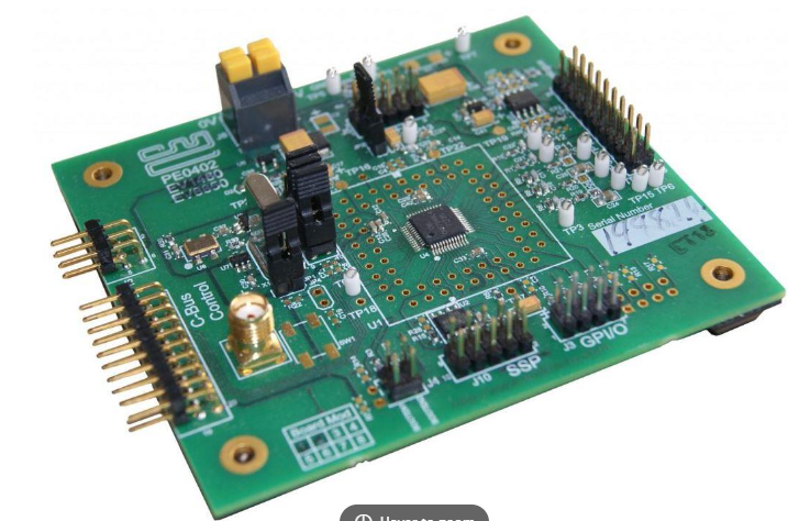 |
The PE0402 Platform Evaluation Kit is designed to assist in the evaluation and application development of the CMX704x/CMX714x range of FirmASIC products. | PE0402_Product_Preview PE0402_User_Manual PE0402_Schematics |
|
PE0003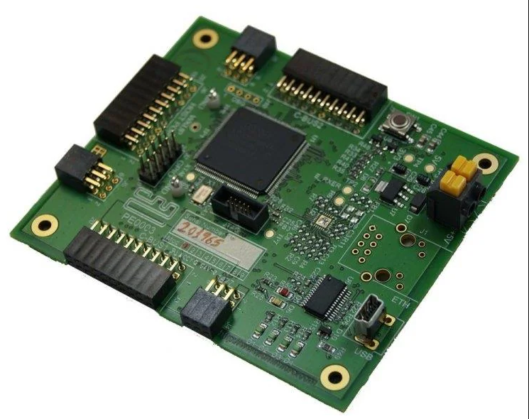 |
The PE0003 Evaluation Kit Interface Card is a global interface system for use with evaluation kits for CML’s new generation ICs, including FirmASIC™ based products. This greatly simplifies the approach to the evaluation and design-in process. | PE0003_Product_Page | |