RF Building Blocks
CMX994/994A/994E/994G – RF Direct Conversion Receiver ICs
The CMX994, CMX994A, CMX994E, CMX994G is a family of direct conversion receiver ICs with PowerTrade™; the ability to dynamically select power against performance modes to optimise operating trade-offs.
CMX994 – Standard and low power modes
CMX994A – Standard and additional low power modes
CMX994E – Enhanced, standard and low power modes
CMX994G – Enhanced, standard and low power modes, 30MHz guaranteed performance
The CMX994/A/E/G offer exceptional blocking performance, typical values are in the range 98dB to 102dB depending on the measurement method. All three devices include a broadband LNA with gain control followed by a high dynamic range, very high IIP2, I/Q demodulator. The receiver baseband section includes amplifiers and precise, configurable bandwidth, baseband filter stages. LO generation is provided by an integer-N PLL and a VCO negative resistance amplifier; an external LO may also be used. LO dividers are provided for flexible multi-band operation.
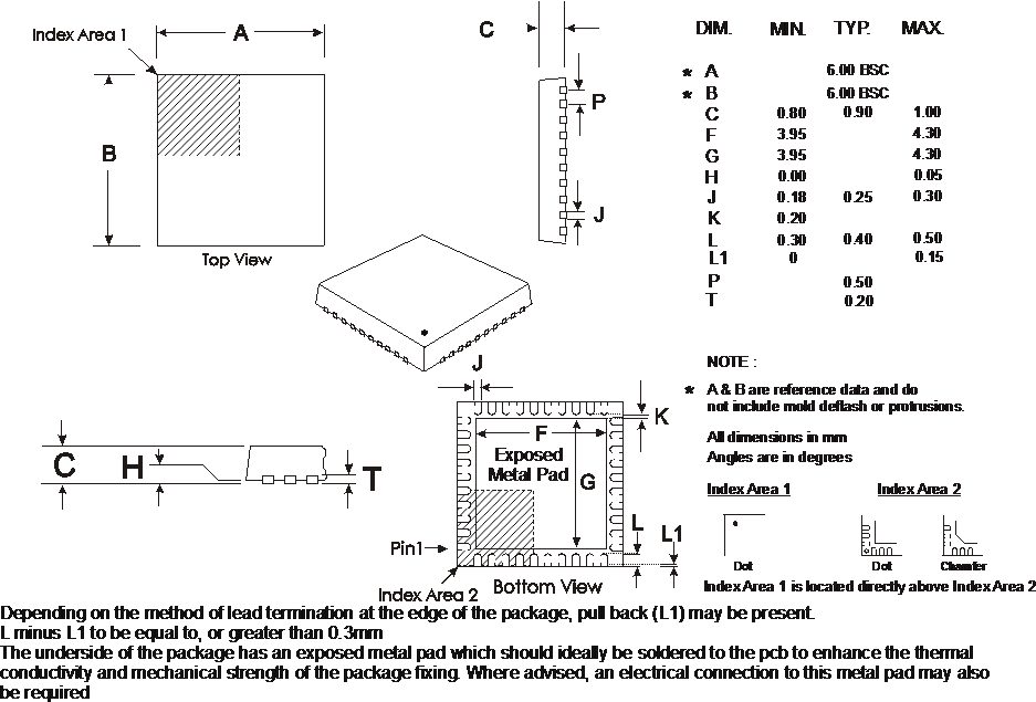
The CMX994/A/E/G operates from a single 3.3V supply over a temperature range of –40°C to +85°C and are available in a small 40-pin VQFN (Q4) package.
Devices are available through our Distributor Network.

Features
- Direct Conversion Receiver Family with PowerTrade™ Flexible Power vs. Performance Modes – CMX994 – Standard and Low Power Modes – CMX994A – Standard and Additional Low Power Modes – CMX994E – Enhanced, Standard and Low Power Modes – CMX994G – Enhanced, Standard and Low Power Modes, 30MHz guaranteed performance for radios operating down to 30MH
- Rx Single Conversion to Zero IF, Near-zero IF or Low IF; Zero IF Eliminates Image Responses
- Very High Mixer IIP2 for Practical Zero IF Receiver
- 100MHz to 1000MHz I/Q Demodulator (CMX994A/E/G) 100MHz to 940MHz I/Q Demodulator (CMX994) Extended Operation down to 50MHz or 30MHz (CMX994G)
- LNA with Gain Control
- Precise Filtering with 1:2:4 Bandwidth Select Control
- Mixer Bandwidth up to 20MHz
- Local Oscillator – LO synthesiser – VCO Negative Resistance Amplifier – Rx LO Divide by 2, 4 or 6 Modes – Tx LO Output with Divide by 1, 2, 4 or 6 Modes
- Small Size 40-pin VQFN Package
Applications
- Analogue/digital Multi-mode Radio
- Software Defined Radio (SDR)
- Data Telemetry Modems
- Satellite Communications
- Constant Envelope and Linear Modulation
- Rx Function Compatible with CMX998
- Cartesian Feedback Loop Transmitter
- Narrowband e.g.: 25kHz, 12.5kHz and 6.25kHz
- Wideband Data e.g. >1MHz Bandwidth
Power Supply Requirement
- 3.0 to 3.6 V
Downloads
Design Resources
CMX994 FAQ
Q, Are the CMX994A, CMX994E and CMX994G devices pin compatible with the CMX994 in my digital radio?
A, Yes all four devices are pin and function compatible. However, if the CMX994A, CMX994E or CMX994G are to be fitted into an existing CMX994 design, it is recommended that the new extended DC Offset register is used.
There are additional benefits in adopting the CMX994A, CMX994E and CMX995G they include additional low power operating modes, enhanced mixer IM capability and guaranteed 30MHz operation, these are illustrated below. A means of confirming device type by a software read is also shown.
| Register Name | Register bit | Name | CMX994 | CMX994A | CMX994E | CMX994G | Notes | |
| Options Control - $15 Read from - $E5 |
b7 | IP3X | x | x | Enhanced Mixer Intermodulation | Power consumption increase by 10mA typ | ||
| b3 | PDQ | x | Power down entire Q receive path. I enabled | 9mA typ saved | ||||
| b2 | PDI | x | Power down entire I receive path, Q enabled | 9mA typ saved | ||||
| b1..0 | PHCON/PHOFF | x | LO Phase Correction power down bits | 14mA typ saved | ||||
| Extended Rx Offset - $17 Read from - $E7 |
b13..8 | QDC5..QDC0 | x | Q path extended DC offset correction | Compensation range increased from +-175mV to +-775mV in 25mV steps | |||
| b5..0 | IDC5..IDC0 | x | I path extended DC offset correction | |||||
| Guaranteed 30MHz Operation | x | x | x | x | x | Yes | IP3, Image Rejection and IQ Balance performance at 30MHz | |
| PLL M Divider - $D2 Read only. | b4,b2 | ID1, ID2 | 00 | 01 | 10 | 10 | Device identification bits; 11 is reserved. | |
Q. Adjacent channel performance is not as good as I had expected even when applying large DC offset compensation on an unmodified EV994AE Evaluation Kit.
A. For optimal performance the CMX994A/E PLL frequency should be centred on the wanted channel. If it is not, then issues relating to DC Offsets and Adjacent Channel Performance will be encountered. This is documented on the EV9942AE User Manual, section 6.5.2. Receiver Operation.
The 19.2 MHz reference for the CMX994A/E PLL is sourced from a Golledge GTXO-83 VCTCXO as shown below.

To operate within the ppm quoted frequency limits the GTXO-83 should be biased to 1.5V as a Vcc of 3V is used. As can be seen from the EV9942AE schematic extract above the biasing of the ADJ input pin is set by two resistors, R18 and R21. This is correct for a supply voltage of 3V as R18 and R21 set the bias voltage to 3 / 2 = 1.5V. However, as the EV994AE default supply is 3.3V therefore the resistors R18 and R21 will set the bias voltage to 1.65V, outside of the quoted specifications.
Therefore, for best performance using a 3.3V supply, R18 and R21 should be replaced with 8K87@1% and 10K7@1% resistors giving an ADJ bias of 1.496V, bringing the reference frequency into specification. This results in a smaller DC offset that may be removed by using the CMX994AE Receive Offset Register.
Frequency Estimation for a VCO using a Negative Resistance Amplifier
Application Note describing how to estimate the operating frequency of VCO designs using a negative resistance amplifier. An Excel spreadsheet that automates the calculation is available below.
Excel Spreadsheet - Frequency Estimation for a VCO using a Negative Resistance Amplifier
An Excel spreadsheet that calculates the operating frequency of VCO designs using a negative resistance amplifier. An Application Note describing the process is available above.
CMX994/A/E Interference Immunity
Through clarification of blocking and second order intermodulation performance, together with empirical measurement, this app note illustrates the excellent characteristics of the CMX994/CMX99A/CMX994E marking its suitability for professional radio designs.
CMX994A / CMX994E 400MHz to 470MHz Operation
An Application Note demonstrating through the use of a simple RF matching circuit for the CMX994A and CMX994E devices in 400MHz to 470MHz band applications. Comparative measurements are made with the existing EV9942A/E and DE9945A Evaluation Boards throughout and results provided.
CMX994/A/E LNA Performance and Applications
An application note that describes the performance characteristics of the CMX994’s LNA and the benefits of this device for typical PMR radio designs.
CMX994 - Demonstration Video Scripts
These scripts are used in the "CMX994 Demonstration" video. The scripts guide the user through Tx/Rx frequency trimming, Rx I/Q DC offset calibration, Rx Equalizer training, Tx I/Q DC offset calibration, and formatted data transfer.
| DE9941A | The DE9941A is a credit-card sized, fully functional, UHF wireless data modem using the CMX994E Direct Conversion Receiver, the CMX998 Cartesian Feedback Loop Transmitter and the CMX7364 High Performance Multi-mode Wireless Data Modem. Full design data and test scripts are available to download from the DE9941A Product Page. | DE9941A_Product_Page |
| EV9942A/9942E | Two versions of the Evaluation Kit are available allowing the user to investigate all aspects of the chosen CMX994, high-performance direct conversion receiver. A common PC-based application identifies the CMX994 version and starts an interactive GUI for configuration and control. A separate hi-res schematic is available for both versions of the EV9942. | EV9942_Product_Preview
|
C-BUS Guides
Guides to operation and interfacing
EV9942 Evaluation Software
A common GUI-based application for the EV9942/EV9942A/EV9942E Evaluation Kits. A PE0003 Universal Interface Card is required to use this application. Version 4.1
EV9942 Quick Start
A simple guide to help users get started evaluating the EV9942, EV9942A and EV9942E Evaluation Kits. Ver.2
EV9942A Board Schematics
EV9942A Board high-resolution schematic. Ver.A03
EV9942E Board Schematics
EV9942E Board high-resolution schematic. Ver.A02
PE0003 Driver
PE0003 USB driver for Windows. Version 1.0
EV9942A BOM
EV9942A Board BOM Ver.A03
EV9942E BOM
EV9942A Board BOM Ver.A02